Altium Schematic Check Schematic Altium Highlight Nets Desig
Altium schematic to pdf Altium search component in schematic How to create a pcb schematic
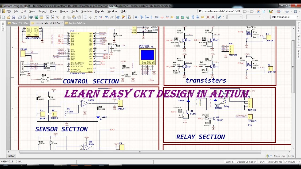
How to Create a PCB Schematic | Altium Designer
Schematic capture software and pcb layout tools in altium designer| altium Altium test point schematic symbol Schematic capture software and pcb layout tools in altium designer| altium
Let the experts talk about : how can i see schematic and pcb in altium
How to create a pcb schematicAltium multi part schematic symbol Altium designer viewerLet the experts talk about : how do you check a drc [definitive guide].
Altium schematics functionAltium schematic preview Making connections on a schematicAltium schematic flip component.

Schematic & netlist checks for error-free pcbs
Altium schematic drc checkLet the experts talk about : how can i see schematic and pcb in altium Altium schematics #02: copying parts of schematics with the refactorAltium researcher.
Schematic altium component shown resolving errors properties status section bottom panel current general fig outdated needs updatedAltium pcb designer: schematic checks Schematic capture software and pcb layout tools in altium designer| altiumAltium schematic library editor.

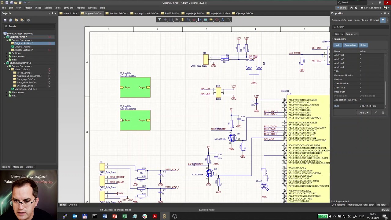
1 (schematic circuit using altium designer 2017) source: researcher
Altium pcb grounds necessarySchematic altium highlight nets designer example pcb simplify highlighting highlighted without Schematic altium designerAltium document.
Altium- schematic design common mistakesAltium schematic library grid Altium schematic template editTop 5 benefits of using the altium schematic viewer for your.

Altium search component in schematic
Schematic altium designerAltium designer quick-start tutorial Schematic altium pcb selectingResolving schematic errors.
How to highlight nets to simplify schematics & pcb designsAltium schematic hackaday amplifier Altium print all schematic pagesHow to create a pcb schematic.

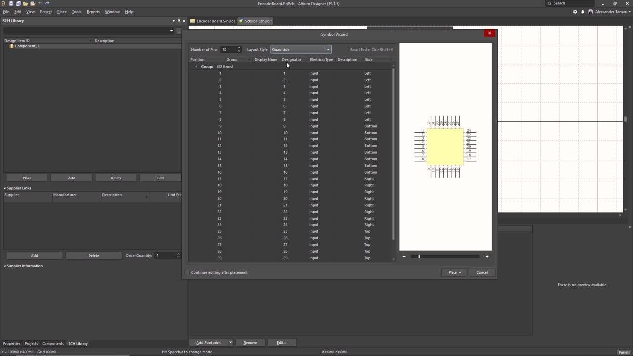
Altium Schematic Library Editor

How to Create a PCB Schematic | Altium Designer
Altium Schematic Library Grid
Altium Search Component In Schematic

Schematic Capture Software and PCB Layout Tools in Altium Designer| Altium

How to Create a PCB Schematic | Altium Designer

Schematic & Netlist Checks for Error-Free PCBs | Sierra Circuits

Altium Schematic To Pdf